⚡ When the Compiler Is a PCB Factory
TL;DR: A PCB factory isn’t a printer—it’s a compiler that recompiles your board through its own software and emails you to approve the diff. I spent a week braced for it to quietly change my design; the design was fine. What actually bricked all five boards was a bug in my own firmware—a clock-cycle assumption that the chip’s flash wait states silently broke.
On August 3, 2026, an engineer at JLCPCB emailed me about Semaphore, the little USB-C status-light board I have been building. The message said, “We have made modification for D4.”
That was alarming because I had already told them D4 was correct. JLC had sent me a component-placement render on July 30 asking me to confirm five LEDs and two chips. I checked it against my KiCad board and placement file, specifically called out D4’s unusual rotation, and approved production. They acknowledged that and said they would proceed. Four days later, a different engineer sent a new render saying D4 had been modified.
The new render appeared to straighten D4 to 0°, matching its three neighbors instead of the -90° in my placement file. I still do not know whether a person changed it, an automated rotation table normalized it, or something else happened inside JLC’s process. From outside, I can only see that the compiled output changed.
The change looks sensible if you treat the board as a picture. Four SK6805-EC15 addressable RGB LEDs sit in a row on Semaphore, and D4 is the only one rotated 90 degrees. It resembles a typo. In the circuit, though, the rotation is intentional.
If D4 were straightened to 0°, its data input would land on 5 volts, its power pin on a data trace, its data output on ground, and its ground pin on the preceding LED’s output. The package is a square with four pads at the corners, so it would still sit neatly on the board. Every pin would land on copper. The soldering could look perfect while the circuit was electrically wrong.
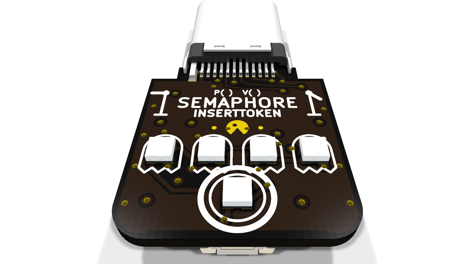
Semaphore rev F. D4 is the third small LED from the left—rotated 90 degrees from its three identical neighbors, on purpose.
I refused the change and asked JLC to state the before-and-after rotation in degrees. The order moved forward from there.
I Thought the Factory Printed the File
I am new to PCB design. Until this summer, my vague mental model was that I would finish a board in KiCad, upload it to a factory, and the factory would manufacture what was on the screen. Something like sending a PDF to a print shop, except the printer uses fiberglass and copper.
KiCad is closer to a source-code editor. From it I export Gerbers for the copper, solder mask, and silkscreen; drill files for the holes; a bill of materials for the parts; and a component-placement list for their positions and rotations. KiCad describes Gerbers as manufacturing outputs and position files as inputs commonly used to program pick-and-place machines.[1]
Those exports are not the exact instructions that run JLC’s machines. JLC says an engineer generates a production file from the customer’s Gerbers according to the factory’s capabilities and rules, then asks the customer to compare that version with the original.[2] For assembly, its system matches parts from the BOM, while placement is finalized from the CPL and PCB silkscreen; JLC tells customers to make sure the BOM, CPL, PCB, and orientation markings agree.[3]
The pipeline looks something like this:
intent
  → KiCad schematic and board
  → Gerber + drill + BOM + placement files
  → factory CAM and assembly data
  → panelized board + machine placements
  → physical PCB
I think of the middle as compilation now. The KiCad project is source. Gerber, BOM, and placement data function like an intermediate representation. The factory has a backend for its specific machines, tolerances, part library, panel sizes, and process rules. The manufactured board is the executable—except this compiler occasionally emails you.
A Human Somewhere in the Loop
A software compiler has a language specification. If the source is well-defined, I generally expect the same semantics after compilation. There are bugs and target differences, of course, and C programmers have spent decades learning what happens when the source leaves room for interpretation. But nobody at Clang normally opens my file, decides one line looks odd, and rewrites it to match the neighboring lines.
PCB manufacturing has more interpretation at its boundaries. A Gerber describes shapes, not why those shapes exist. A placement file gives an angle, but that angle still has to line up with a footprint convention, a component model, a package mark, the factory’s coordinate system, and whatever software or person reviews the result. Silkscreen can provide a clue, but it is another artifact that can disagree with the others.
Semaphore’s D4 sat in that gap. Its correct orientation differed from its identical neighbors, and the physical package’s visible mark is near pin 3 rather than pin 1. Whoever or whatever flagged it—an engineer, a rotation table in a part library, I do not know yet—was presumably trying to prevent a placement error and may have created one instead.
The output can therefore be structurally valid—the component fits on all four pads—while its meaning is wrong. I can recompile, but hardware makes that loop expensive. A bad software build wastes a few minutes. A bad PCB spin costs money, shipping, components, and at least another week, and it leaves me with five copies of the misunderstanding.
AI Lowered the Design Barrier
I probably would not have discovered any of this yet without AI. PCB design was one of those fields I had mentally filed under “learn someday.” The electrical rules are only part of it. There is KiCad, footprint construction, routing, part sourcing, fabrication tolerances, assembly constraints, and an impressive vocabulary of file formats and acronyms. Even getting to the point where I could make a plausible mistake required a lot of specialized knowledge.
The current generation of AI models changed that threshold for me. On Semaphore, they read datasheets, edited KiCad board files, and helped me build project-specific manufacturing checks. They helped write a geometry-aware router for the last airwires—the connections still left unrouted. When JLC’s design-for-manufacturing (DFM) check caught overlapping same-net vias that KiCad had allowed, we turned that factory warning into a regression test. Rev F eventually reached zero design-rule violations and passed every automated manufacturing check I knew to run, despite my never having taken a PCB through production before.
AI made the design legible enough for me to enter the factory process. It did not make the process disappear. If anything, it exposed the parts that software people are least trained to notice: the informal contract between two toolchains, the visual conventions that carry electrical meaning, and the judgment applied after the files leave your computer.
I wrote earlier that verification is the bottleneck once AI makes generation cheap. PCBs are an unusually literal version of that. The design can be regenerated in minutes. The next verification step involves another company, production equipment in another country, a package in the mail, a microscope, a current-limited power supply, and eventually five boards sitting on my desk.
Review the Compiled Output
I have started treating a PCB order less like uploading a finished design and more like handing source to an unfamiliar compiler.
I keep hashes of the exact Gerber, BOM, and placement files I uploaded. I pay for production-file confirmation. I compare the factory output to my own source rather than to an earlier factory preview. For polarized parts, I verify pin 1 against actual nets and nearby landmarks instead of trusting that two pictures look alike. If a factory changes something, I want the proposed edit stated numerically—not described as “corrected.”
The review loop is not a safety net bolted onto manufacturing; it is how manufacturing works. My board can pass KiCad’s checks, pass my own scripts, render beautifully, upload successfully, and still be waiting for one last semantic decision inside the factory.
I wanted AI to help me turn software into hardware. It did, and along the way it taught me that hardware has source code, intermediate representations, compiler quirks, and code review. Meanwhile, the order has moved forward and I am waiting for the boards. The next review will not be another image on a screen; it will be physical bring-up. If all goes well, the final merge will arrive in a cardboard box.
The Boards Arrived
The box showed up a few weeks later. D4 sat in its correct -90° orientation—the factory-compile problem I had braced for never happened. The board JLC built was fine.
The bug was mine.
I plugged in the first board and all five LEDs lit solid white and stayed there. Every color command I sent updated the device’s internal state and changed nothing physical. I assembled a second board by hand, independently, and it failed the exact same way—five lamps, solid white, identical. Two boards failing identically is the textbook signature of a systemic manufacturing defect: a bad footprint, a wrong part, a rotation propagated across the panel. So that is where I spent days looking—cold solder joints, counterfeit LEDs, a marginal ground under the microcontroller. None of it was the problem.
The real cause was a mismatch between my source and the silicon that ran it. These addressable LEDs read bits as pulse widths—a short high pulse is a zero, a long one is a one—and each pulse has to land inside a window a few hundred nanoseconds wide. I hit that window with hand-counted NOP instructions, assuming one clock cycle each. But code fetched from this chip’s flash runs with two mandatory wait states at 48 MHz, so my delay loops ran roughly one-and-a-half to three times slower than I had counted. Every zero overran the window and decoded as a one. Every pixel latched to all-ones—0xFFFFFF, solid white. Identical silicon stretches identically, which is exactly why two hand-built boards failed the same way with no shared defect between them.
That is a compiler bug in everything but name. The source was correct against the abstract machine in my head—one cycle per instruction—and wrong against the real target, whose execution model I had never actually reviewed. The fix was to move the timing-critical routine out of flash and into RAM, where instruction fetch has no wait states and my cycle counts came true again. I reflashed, and the LEDs came up in the colors I asked for. First real frame: one zone green, the pilot lamp white.
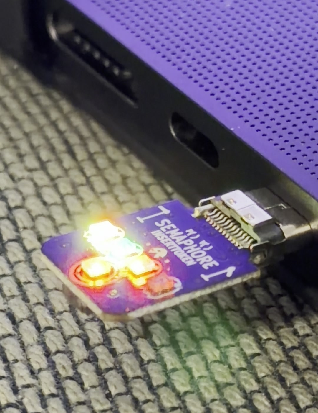
The first board, alive on its own 5 volts and finally decoding frames—caught here mid-cycle in an amber alert state. For three days, every one of those LEDs had been stuck solid white.
So the essay braced for the wrong compiler. I spent a week worried the factory would silently rewrite my board, and the board was perfect. What actually bit me was the other compiler in the pipeline—the one that turns C into instructions and instructions into timing on a specific die—and a target quirk I never checked. Hardware has everything I listed above: source code, intermediate representations, compiler quirks, code review. It has undefined behavior too, and the debugger for it is an oscilloscope you only think to reach for once you’ve eliminated everything you can see.
The boards work now. The final merge did arrive in a cardboard box—it just needed one more patch before it built clean.
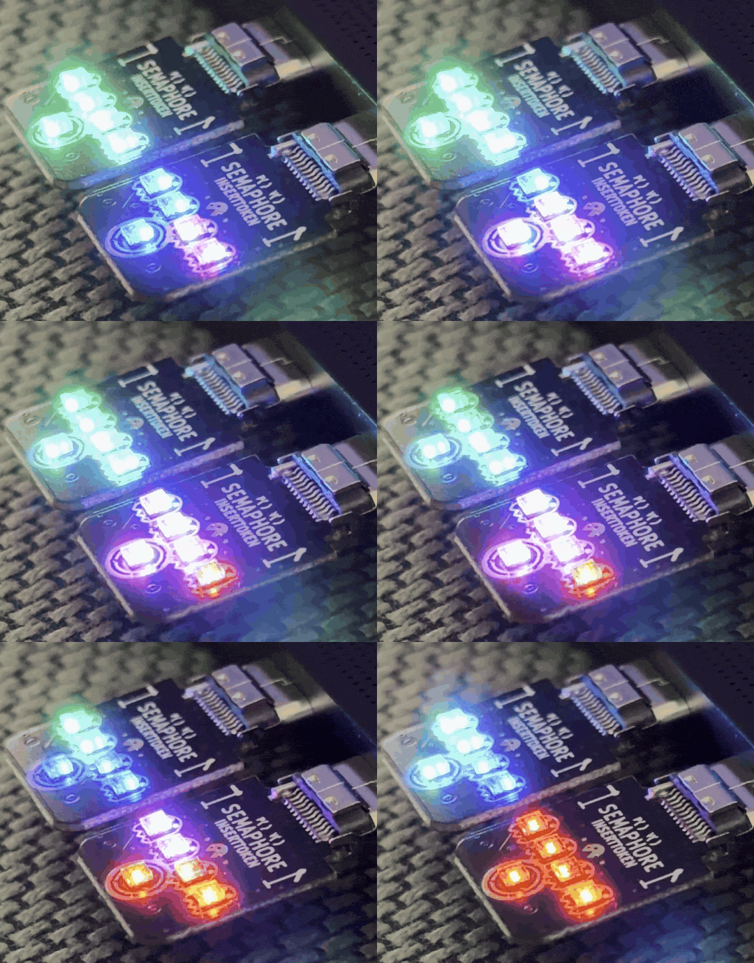
Two boards, each addressed to its own colors and changing independently. A week earlier, both were stuck identically white.
Citations
[1] KiCad PCB Editor documentation: generating manufacturing outputs — KiCad ↩
[2] How to confirm the production file? — JLCPCB, updated April 24, 2025 ↩
[3] Common PCBA after-sales issues and FAQ — JLCPCB, updated May 16, 2026 ↩
> TL;DR: A PCB factory isn't a printer—it's a compiler that recompiles your board through its own software and emails you to approve the diff. I spent a week braced for it to quietly change my design; the design was fine. What actually bricked all five boards was a bug in my own firmware—a clock-cycle assumption that the chip's flash wait states silently broke.
On August 3, 2026, an engineer at JLCPCB emailed me about Semaphore, the little USB-C status-light board I have been building. The message said, "We have made modification for D4."
That was alarming because I had already told them D4 was correct. JLC had sent me a component-placement render on July 30 asking me to confirm five LEDs and two chips. I checked it against my KiCad board and placement file, specifically called out D4's unusual rotation, and approved production. They acknowledged that and said they would proceed. Four days later, a different engineer sent a new render saying D4 had been modified.
The new render appeared to straighten D4 to `0°`, matching its three neighbors instead of the `-90°` in my placement file. I still do not know whether a person changed it, an automated rotation table normalized it, or something else happened inside JLC's process. From outside, I can only see that the compiled output changed.
The change looks sensible if you treat the board as a picture. Four SK6805-EC15 addressable RGB LEDs sit in a row on Semaphore, and D4 is the only one rotated 90 degrees. It resembles a typo. In the circuit, though, the rotation is intentional.
If D4 were straightened to `0°`, its data input would land on 5 volts, its power pin on a data trace, its data output on ground, and its ground pin on the preceding LED's output. The package is a square with four pads at the corners, so it would still sit neatly on the board. Every pin would land on copper. The soldering could look perfect while the circuit was electrically wrong.

Semaphore rev F. D4 is the third small LED from the left—rotated 90 degrees from its three identical neighbors, on purpose.
I refused the change and asked JLC to state the before-and-after rotation in degrees. The order moved forward from there.
## I Thought the Factory Printed the File
I am new to PCB design. Until this summer, my vague mental model was that I would finish a board in KiCad, upload it to a factory, and the factory would manufacture what was on the screen. Something like sending a PDF to a print shop, except the printer uses fiberglass and copper.
KiCad is closer to a source-code editor. From it I export Gerbers for the copper, solder mask, and silkscreen; drill files for the holes; a bill of materials for the parts; and a component-placement list for their positions and rotations. KiCad describes Gerbers as manufacturing outputs and position files as inputs commonly used to program pick-and-place machines.<sup><a href="#cite-1" id="ref-1">[1]</a></sup>
Those exports are not the exact instructions that run JLC's machines. JLC says an engineer generates a production file from the customer's Gerbers according to the factory's capabilities and rules, then asks the customer to compare that version with the original.<sup><a href="#cite-2" id="ref-2">[2]</a></sup> For assembly, its system matches parts from the BOM, while placement is finalized from the CPL and PCB silkscreen; JLC tells customers to make sure the BOM, CPL, PCB, and orientation markings agree.<sup><a href="#cite-3" id="ref-3">[3]</a></sup>
The pipeline looks something like this:
```
intent
→ KiCad schematic and board
→ Gerber + drill + BOM + placement files
→ factory CAM and assembly data
→ panelized board + machine placements
→ physical PCB
```
I think of the middle as compilation now. The KiCad project is source. Gerber, BOM, and placement data function like an intermediate representation. The factory has a backend for its specific machines, tolerances, part library, panel sizes, and process rules. The manufactured board is the executable—except this compiler occasionally emails you.
## A Human Somewhere in the Loop
A software compiler has a language specification. If the source is well-defined, I generally expect the same semantics after compilation. There are bugs and target differences, of course, and C programmers have spent decades learning what happens when the source leaves room for interpretation. But nobody at Clang normally opens my file, decides one line looks odd, and rewrites it to match the neighboring lines.
PCB manufacturing has more interpretation at its boundaries. A Gerber describes shapes, not why those shapes exist. A placement file gives an angle, but that angle still has to line up with a footprint convention, a component model, a package mark, the factory's coordinate system, and whatever software or person reviews the result. Silkscreen can provide a clue, but it is another artifact that can disagree with the others.
Semaphore's D4 sat in that gap. Its correct orientation differed from its identical neighbors, and the physical package's visible mark is near pin 3 rather than pin 1. Whoever or whatever flagged it—an engineer, a rotation table in a part library, I do not know yet—was presumably trying to prevent a placement error and may have created one instead.
The output can therefore be structurally valid—the component fits on all four pads—while its meaning is wrong. I can recompile, but hardware makes that loop expensive. A bad software build wastes a few minutes. A bad PCB spin costs money, shipping, components, and at least another week, and it leaves me with five copies of the misunderstanding.
## AI Lowered the Design Barrier
I probably would not have discovered any of this yet without AI. PCB design was one of those fields I had mentally filed under "learn someday." The electrical rules are only part of it. There is KiCad, footprint construction, routing, part sourcing, fabrication tolerances, assembly constraints, and an impressive vocabulary of file formats and acronyms. Even getting to the point where I could make a plausible mistake required a lot of specialized knowledge.
The current generation of AI models changed that threshold for me. On Semaphore, they read datasheets, edited KiCad board files, and helped me build project-specific manufacturing checks. They helped write a geometry-aware router for the last airwires—the connections still left unrouted. When JLC's design-for-manufacturing (DFM) check caught overlapping same-net vias that KiCad had allowed, we turned that factory warning into a regression test. Rev F eventually reached zero design-rule violations and passed every automated manufacturing check I knew to run, despite my never having taken a PCB through production before.
AI made the design legible enough for me to enter the factory process. It did not make the process disappear. If anything, it exposed the parts that software people are least trained to notice: the informal contract between two toolchains, the visual conventions that carry electrical meaning, and the judgment applied after the files leave your computer.
I wrote earlier that [verification is the bottleneck](/verification-is-the-bottleneck.md) once AI makes generation cheap. PCBs are an unusually literal version of that. The design can be regenerated in minutes. The next verification step involves another company, production equipment in another country, a package in the mail, a microscope, a current-limited power supply, and eventually five boards sitting on my desk.
## Review the Compiled Output
I have started treating a PCB order less like uploading a finished design and more like handing source to an unfamiliar compiler.
I keep hashes of the exact Gerber, BOM, and placement files I uploaded. I pay for production-file confirmation. I compare the factory output to my own source rather than to an earlier factory preview. For polarized parts, I verify pin 1 against actual nets and nearby landmarks instead of trusting that two pictures look alike. If a factory changes something, I want the proposed edit stated numerically—not described as "corrected."
The review loop is not a safety net bolted onto manufacturing; it is how manufacturing works. My board can pass KiCad's checks, pass my own scripts, render beautifully, upload successfully, and still be waiting for one last semantic decision inside the factory.
I wanted AI to help me turn software into hardware. It did, and along the way it taught me that hardware has source code, intermediate representations, compiler quirks, and code review. Meanwhile, the order has moved forward and I am waiting for the boards. The next review will not be another image on a screen; it will be physical bring-up. If all goes well, the final merge will arrive in a cardboard box.
## The Boards Arrived
The box showed up a few weeks later. D4 sat in its correct `-90°` orientation—the factory-compile problem I had braced for never happened. The board JLC built was fine.
The bug was mine.
I plugged in the first board and all five LEDs lit solid white and stayed there. Every color command I sent updated the device's internal state and changed nothing physical. I assembled a second board by hand, independently, and it failed the exact same way—five lamps, solid white, identical. Two boards failing identically is the textbook signature of a systemic manufacturing defect: a bad footprint, a wrong part, a rotation propagated across the panel. So that is where I spent days looking—cold solder joints, counterfeit LEDs, a marginal ground under the microcontroller. None of it was the problem.
The real cause was a mismatch between my source and the silicon that ran it. These addressable LEDs read bits as pulse widths—a short high pulse is a zero, a long one is a one—and each pulse has to land inside a window a few hundred nanoseconds wide. I hit that window with hand-counted `NOP` instructions, assuming one clock cycle each. But code fetched from this chip's flash runs with two mandatory wait states at 48 MHz, so my delay loops ran roughly one-and-a-half to three times slower than I had counted. Every zero overran the window and decoded as a one. Every pixel latched to all-ones—`0xFFFFFF`, solid white. Identical silicon stretches identically, which is exactly why two hand-built boards failed the same way with no shared defect between them.
That is a compiler bug in everything but name. The source was correct against the abstract machine in my head—one cycle per instruction—and wrong against the real target, whose execution model I had never actually reviewed. The fix was to move the timing-critical routine out of flash and into RAM, where instruction fetch has no wait states and my cycle counts came true again. I reflashed, and the LEDs came up in the colors I asked for. First real frame: one zone green, the pilot lamp white.

The first board, alive on its own 5 volts and finally decoding frames—caught here mid-cycle in an amber alert state. For three days, every one of those LEDs had been stuck solid white.
So the essay braced for the wrong compiler. I spent a week worried the factory would silently rewrite my board, and the board was perfect. What actually bit me was the other compiler in the pipeline—the one that turns C into instructions and instructions into timing on a specific die—and a target quirk I never checked. Hardware has everything I listed above: source code, intermediate representations, compiler quirks, code review. It has undefined behavior too, and the debugger for it is an oscilloscope you only think to reach for once you've eliminated everything you can see.
The boards work now. The final merge did arrive in a cardboard box—it just needed one more patch before it built clean.

Two boards, each addressed to its own colors and changing independently. A week earlier, both were stuck identically white.
## Citations
<p id="cite-1">[1] <a href="https://docs.kicad.org/master/en/pcbnew/pcbnew.html" target="_blank" rel="noopener noreferrer">KiCad PCB Editor documentation: generating manufacturing outputs</a> — KiCad <a href="#ref-1">↩</a></p>
<p id="cite-2">[2] <a href="https://jlcpcb.com/help/article/how-to-confirm-the-production-file" target="_blank" rel="noopener noreferrer">How to confirm the production file?</a> — JLCPCB, updated April 24, 2025 <a href="#ref-2">↩</a></p>
<p id="cite-3">[3] <a href="https://jlcpcb.com/help/article/common-pcba-after-sales-issues-and-faq" target="_blank" rel="noopener noreferrer">Common PCBA after-sales issues and FAQ</a> — JLCPCB, updated May 16, 2026 <a href="#ref-3">↩</a></p>